

Master PCB Design with KiCad 8.0: Complete Beginner’s Guide to Electronics in 2026
Did you know that nearly 80% of electronic prototypes fail on the first try due to poor PCB layout? In 2026, as India’s electronics manufacturing sector grows at over 15% annually, the ability to design a reliable printed circuit board (PCB) is no longer a niche skill — it’s a fundamental requirement for every engineering student, hobbyist, and maker. Whether you’re building a smart IoT sensor for your final-year project or a custom drone controller, the difference between a working device and a frustrating tangle of jumper wires often comes down to a well-designed board.
That’s where KiCad 8.0 steps in. Released in early 2026 with a host of user‑friendly improvements — including a revamped schematic editor, real‑time design‑rule checking, and a unified component library — it has quickly become the go‑to open‑source PCB design tool for beginners in India. Unlike expensive proprietary software, KiCad is completely free, runs on Windows, macOS, and Linux, and now supports advanced features like push‑and‑shove routing and interactive BOM generation. With over 2 million downloads worldwide and a rapidly growing community of Indian makers contributing to its library, there has never been a better time to learn PCB design.
In this complete beginner’s guide, you’ll go from zero to your first manufactured board. We’ll cover everything: setting up your KiCad 8.0 environment, creating a schematic symbol, routing traces with confidence, generating Gerber files, and even ordering prototypes. No prior electronics experience? No problem — I’ll explain each step with real component names and clear visuals, staying true to the hands‑on, practical style that helps beginners succeed. By the end, you’ll not only master PCB design with KiCad 8.0 but also understand how to source genuine components and ready‑to‑build kits for your projects — platforms like TecnoMate offer pre‑tested kits and datasheets that make the transition from design to assembly seamless.
Ready to turn your circuit ideas into physical boards? Let’s dive into the world of KiCad 8.0 and build your first PCB — one trace at a time.
Introduction

Why Learn PCB Design?
Printed Circuit Board (PCB) design is the backbone of modern electronics. Every device you use—from a smartphone to a smart home sensor—relies on a custom PCB to connect components reliably. For Indian students, hobbyists, and aspiring engineers, mastering PCB design opens doors to building professional-grade projects, creating final-year engineering prototypes, and even launching your own hardware product. According to NASSCOM, India’s electronics manufacturing sector is expected to reach $300 billion by 2026, and skilled PCB designers are in high demand. Yet, many beginners are intimidated by the steep learning curve of traditional CAD tools.
Enter KiCad 8.0—a free, open-source, and cross-platform EDA (Electronic Design Automation) suite. Released in early 2024, version 8.0 introduced significant improvements: a revamped symbol editor, better 3D viewer integration, and native support for hierarchical schematics. For beginners, KiCad offers a zero-cost entry into professional PCB design without sacrificing features. It runs on Windows, macOS, and Linux, making it accessible to every student in India using a college lab PC or their own laptop.
What This Guide Covers
This Complete Guide to PCB Design for Beginners will walk you through the entire process using KiCad 8.0—from setting up your first project to generating Gerber files for manufacturing. You’ll learn:
- How to navigate the KiCad interface (Eeschema, Pcbnew, Gerbview)
- Creating schematic diagrams with real components (resistors, capacitors, ICs)
- PCB layout fundamentals: footprint assignment, routing, ground planes
- Design rule checks (DRC) and exporting for fabrication
- Practical tips for India-based sourcing of components and PCB fabrication
By the end, you’ll be able to design a simple through-hole or SMD PCB and order it from domestic PCB manufacturers like PCB Power or JLCPCB (which ships to India reliably).
Why KiCad 8.0 for Indian Beginners?
KiCad 8.0’s latest features address pain points for Indian makers:
- Improved library management: Over 50,000 preloaded symbols and footprints, including many Indian-favored components (e.g., Arduino Nano, ESP8266, LM358).
- Built-in component calculator: Helps you determine trace widths for your project’s current requirements—critical when designing power distribution for IoT devices.
- Real-time DRC: Catches footprint mismatch errors early, saving money on faulty prototype boards.
And because PCB design is useless without components, platforms like TecnoMate (India’s marketplace for DIY electronics & engineering project kits) provide genuine parts with datasheets, ready-to-build project kits, and step-by-step guides. You can source tested Arduino, ESP32, sensor modules, and even pre-designed PCB kits from TecnoMate, all with free delivery across India on orders above ₹999. This makes transitioning from design to real hardware seamless—no more hunting for reliable suppliers.
A Note on the Indian Ecosystem
In India, PCB prototyping costs have dropped dramatically. A standard 5cm × 5cm two-layer board costs around ₹200–₹500 from domestic fabs, with lead times of 5–7 days. However, beginners often struggle with incorrect footprints or missing component datasheets. That’s where a structured design flow helps. KiCad 8.0’s PCB calculator and 3D viewer let you visually verify component placement before ordering, reducing rework.
What You’ll Build
Throughout this series, we’ll design a practical project: a USB-powered LM358 audio amplifier with volume control. It uses common components (through-hole resistors, capacitors, a potentiometer, and an op-amp) available at any local electronics shop or via TecnoMate’s project kits. By the end, you’ll have a functional PCB design file and the confidence to tackle your own creations.
Let’s dive into KiCad 8.0—your first step toward becoming a PCB design pro.
Background & Context: The Evolution of PCB Design

The Journey from Point-to-Point to Digital Layouts
Understanding the history of Printed Circuit Board (PCB) design is essential before you start designing your own circuits in KiCad 8.0. The evolution from hand-wired assemblies to today’s complex multi-layer boards tells a story of necessity, reliability, and the relentless drive for miniaturization.
The Era of Pairs (Point-to-Point Wiring) In the earliest days of electronics, there were no PCBs. Circuits were constructed by soldering wires directly to "ties" or tags protruding from components like resistors, capacitors, and transformers. This "punto-a-punto" (point-to-point) wiring method was time-consuming and prone to messy tangles. For many electronics enthusiasts in India, this era is still nostalgic, particularly when building classic analog radios or valve amplifiers where large components demanded extensive wiring.
The Invention of the PCB and Prototyping Boards The first printed circuit boards were essentially etched copper sheets. Engineers would paint an image of the circuit in an acid-resistant varnish (like a carbro negative) onto copper-coated laminate and dip it in acid to remove the unwanted copper, leaving behind the traces. While a massive leap forward, this process was frustratingly difficult for beginners without a darkroom and specialized chemicals.
This limitation gave rise to the Stripboard (Veroboard), a perforated sheet with pre-carved copper tracks. This允许 (allowed) makers to build circuits by cutting tracks and soldering components in place without chemical exposure. Although still used for specific RF (Radio Frequency) prototypes, stripboards introduce impedance mismatches and limit the design possibilities compared to modern layer-based rules.
The SMD Revolution and the Need for CAD As the 20th century progressed, the demand for smaller, more reliable devices skyrocketed. This birthed the Surface Mount Device (SMD) era. SMD components, which are tiny and sit directly on the surface of the board, replaced bulky through-hole components. This miniaturization meant that manual routing across a board (connecting components by hand) was physically impossible.
Enter Computer-Aided Design (CAD). Suddenly, a designer’s role shifted from physical soldering to logical layout. Software became the tool of the trade, allowing for precise trace routing, layer management, and automated verification to catch errors before the PCB was even manufactured.
Why Tools Like KiCad 8.0 Matter Today By aligning with tools like KiCad 8.0, modern hobbyists and engineers skip the messy, unpredictable physical prototyping phases. These software suites provide a correct "physical" view of your board before any copper is actually cut. You can simulate trace widths, manage complex multi-layer stacks, and import Gerber files for manufacturing.
To get comfortable with the physical reality behind these digital designs—such as working with FR-4 substrate material and ensuring proper component placement—most makers in India recommend starting with a physical kit, like those available on TecnoMate, which ships fully tested components and real PCB materials with datasheets across the country. This ensures that when you design with KiCad, you understand not just the software, but the hardware constraints you are managing.
Key Developments in KiCad 8.0 (TABLE)
Enhancing the PCB Design Workflow: What’s New in KiCad 8.0
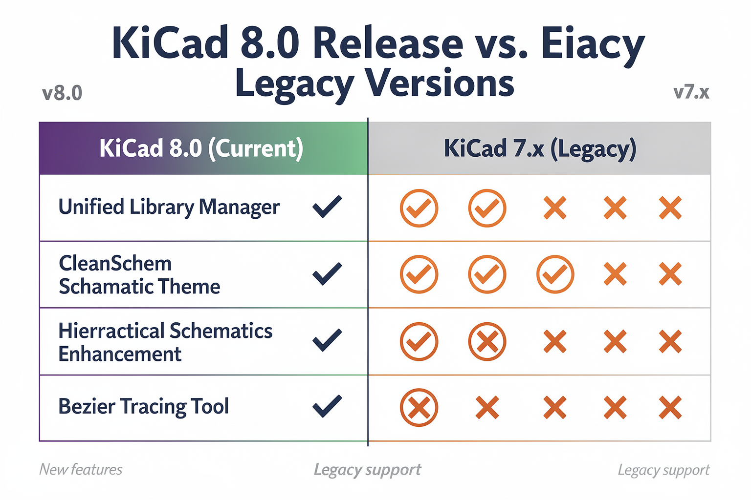
The April 2024 release of KiCad 8.0 represents more than just a numerical update; it is a modernization of the open-source electronics ecosystem, delivering a suite of professional-grade tools that rivaled proprietary software. The core of this evolution lies in the new Engineering Content System (ECS) and strengthened 3D integration, making the software significantly more robust for complex layouts.
For a beginner, navigating the transition from v7 to v8 can be streamlined by understanding exactly where the power has shifted. The architecture now separates schematics, footprints, and 3D models more logically, reducing the friction when assigning physical components to abstract symbols.
Module-Specific Advances
To visualize the scope of these changes, the following table outlines the specific updates across the core modules and their resultant benefits for the average designer.
| Core Module | Version Released | Key New Capability | Beginner Impact |
|---|---|---|---|
| EESchema | 6.0 | Dedicated Integrated 3D Viewer | Allows selection of 3D models and footprint viewing directly in the schematic before routing; prevents stackup errors |
| Pcbnew | 8.0 | Arc Routing Engine | Enables smooth, curved traces instead of only rectangular polygons, simplifying signal integrity design |
| Pcbnew | 8.0 | Touch-Up / Gerber Editing | Lets developers inspect Gerber output files visually within the PCB editor to verify copper pours and masks |
| Pcbnew | 8.0 | Improved Drill Table Logic | Automates the generation and sorting of drill maps, essential for manufacturing accurate holes |
| LayoutEditor | 8.0 | Brush Editor Tools | Provides high-level vector correction tools to quickly tidy up ground pours and copper areas |
Why Arc Routing Matters
Perhaps the most significant "game-changer" for connectors and high-speed designs is the introduction of Arc Routing in Pcbnew 8. In previous versions, sharp 90-degree turns required the use of Rectangular Polygons, which were tedious to place. The new engine handles arcs natively, which is vital for creating the continuous curves found in Mil-spec connectors or for optimizing characteristic impedance in RF traces. Gaining proficiency in KiCad 8 means you are ready to handle projects that require these geometric complexities.
Simplifying 3D Visualization
One persistent pain point for PCB beginners is the disconnect between the 2D schematic and the 3D assembly. KiCad 8 bridges this gap via a dedicated 3D viewer in EESchema. You can now reference generic 3D models or specific "Redwood" models to see exactly how tall a capacitor or resistor is relative to the board edges.
Connecting to the Ecosystem As you learn these features, remember that the software is most powerful when fueled by accurate data. If you are building a project and need precise 3D models or verified schematic libraries that match manufacturers' datasheets perfectly, platforms like TecnoMate provide verified project kits and genuine components across India. Ensuring your KiCad libraries match the physical components you source helps eliminate the "mystery gaps" in your 3D simulations.
The First Step: Installation & Interface
System Requirements and Download
Before you can start laying out your first PCB, you need to get KiCad 8.0 onto your machine. KiCad is completely free and open-source, with no licensing fees or restrictions – a huge advantage over proprietary tools like Altium or Eagle. Version 8.0 introduced a redesigned schematic editor, improved dark mode support, and faster 3D rendering, making it the most beginner-friendly release yet.
Minimum system requirements for KiCad 8.0:
- Windows: 64-bit Windows 10 or later, 4 GB RAM, 2 GB disk space, OpenGL 3.0+
- macOS: macOS 11 Big Sur or later (Intel or Apple Silicon via Rosetta 2)
- Linux: Any modern distro (Ubuntu 20.04+, Fedora 34+, etc.) with GTK 3.24+
💡 If you're on a low‑spec laptop, KiCad runs smoothly even with 4 GB RAM – just avoid opening huge libraries simultaneously.
Step-by-Step Installation
Windows
- Go to kicad.org/download and download the standalone installer for Windows (64-bit).
- Run the installer – accept the default components (Schematic Editor, PCB Editor, 3D Viewer, and Library Manager are all checked).
- During installation, you'll be asked whether to include 3D models. Select "Full Package" (about 1.5 GB) to get footprints for common parts like resistors, capacitors, and connectors.
- After installation, launch KiCad from the Start menu. The first launch may take a few seconds to initialise libraries.
macOS
- Download the
.dmgfile from the official site. Drag the KiCad icon into the Applications folder. - On Apple Silicon Macs, KiCad runs under Rosetta 2 – Apple's translation layer – which has no noticeable performance penalty for PCB design tasks.
- Note: macOS may ask for permission to access files when first opening a project. Grant it.
Linux (Ubuntu/Debian)
- The recommended method is the official KiCad PPA (Personal Package Archive):
sudo add-apt-repository --yes ppa:kicad/kicad-8.0-releases
sudo apt update
sudo apt install kicad
- For other distributions, use Flatpak or AppImage – both are self-contained and auto-update.
First Launch and Interface Overview
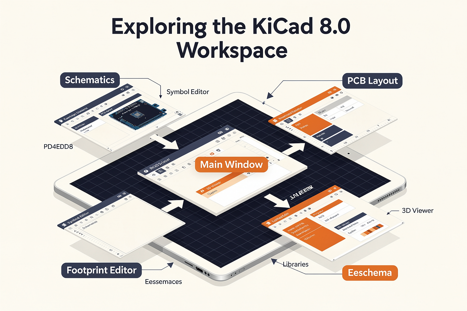
When you open KiCad 8.0, you're greeted by the Project Manager – the hub that organises all files for a single PCB design. At a glance:
- Left sidebar: Your project tree (.kicad_pro project file, schematic, PCB layout, netlist).
- Main toolbar: Shortcuts to open the Schematic Editor (Eeschema), PCB Layout Editor (Pcbnew), Footprint Editor, and Library Manager.
- Recent projects list: Quickly jump back to any design you were working on.
Click the Schematic Editor icon (the green logic gate) to open Eeschema. Here's what you'll see:
- Canvas and grid – draw your circuit using components and wires.
- Right‑hand toolbar – tools for placing symbols, wires, labels, and junctions.
- Top menu – access library management, annotation, and electrical rule checking.
Back in the Project Manager, open the PCB Editor (Pcbnew) – this is where the physical board takes shape. The layout is similar but with layers (copper top, bottom, silkscreen, mask) visible in the right panel.
🧰 TecnoMate tip: Once you've finished your first schematic and PCB layout, you'll need components to prototype. TecnoMate (India's marketplace for DIY electronics) stocks genuine resistors, capacitors, ICs, and connectors with datasheets – perfect for building your KiCad design into a real circuit. They also offer tested project kits that include the exact parts listed in your BOM, so you can avoid sourcing mismatched components.
Key Panels and Tools to Know
- Library Browser – Search through thousands of pre‑built symbols and footprints. KiCad 8.0 now supports fuzzy search, so typing "atmega328" instantly shows the correct symbol.
- Footprint Editor – Customise or create new land patterns. Beginners rarely need this initially, but it's handy for non‑standard parts.
- 3D Viewer – Rotate and inspect your board before manufacturing. KiCad 8.0 added realistic material rendering (copper, solder mask, silkscreen) – a fantastic way to catch clearance errors visually.
Ready to Go
Installation takes about 10 minutes, and the interface is deliberately sparse – only what you need is shown. In the next section we'll create your first schematic symbol and build a simple LED circuit. By the end of this guide, you'll have converted that design into a real PCB that you can order from manufacturers – and source the components for, with confidence, from platforms like TecnoMate.
In-Depth: Creating Your First Schematic
Setting Up the Schematic Canvas
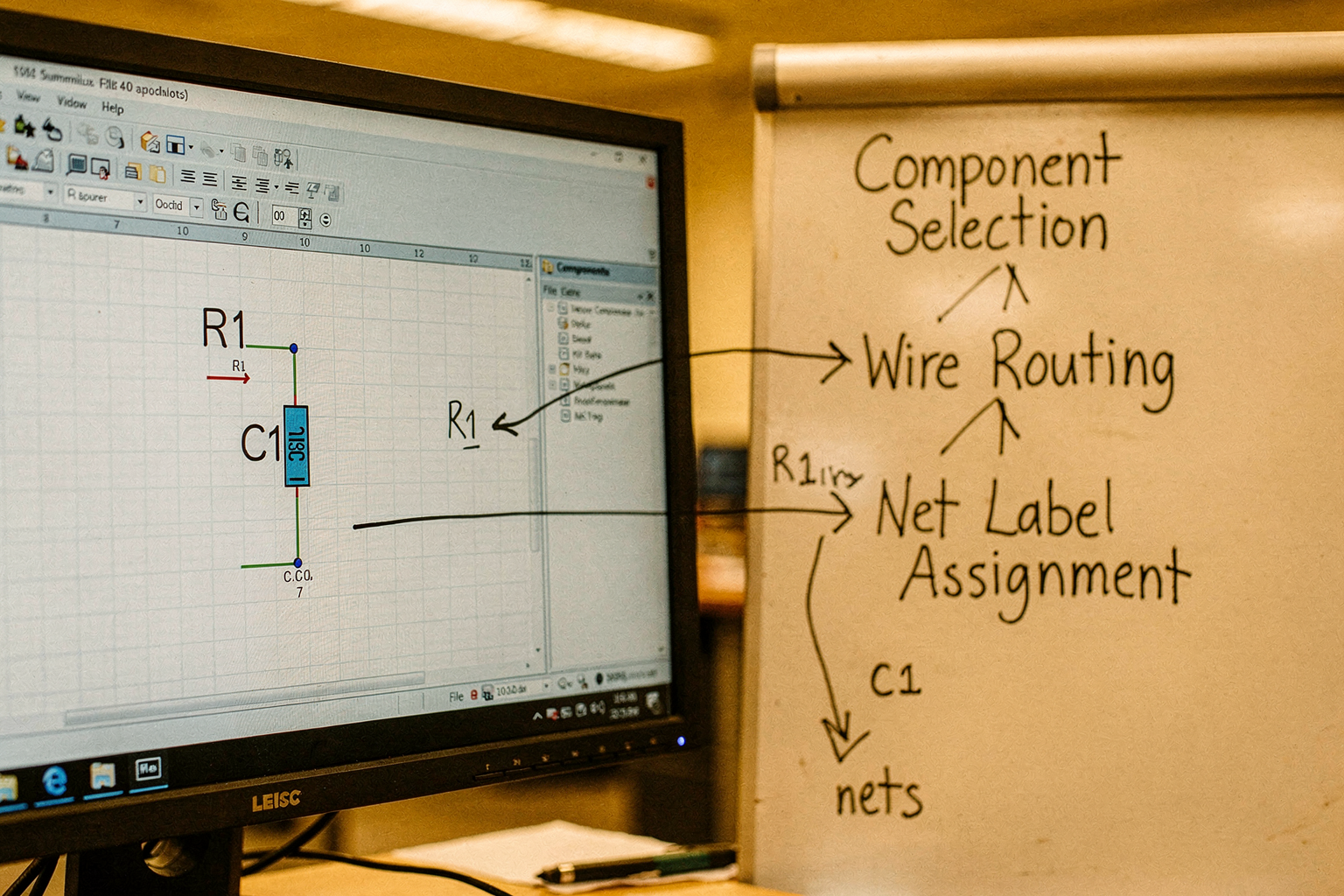
Entering the schematic editor in KiCad 8.0 marks the transition from concept to logic. Start by opening the eeschema environment; the workspace is divided into a schematic window and the library manager. The default configuration usually sets up a standard A4 sheet, which is ideal for printing high-quality schematics in India, though you can switch to Letter size if local standards dictate differently. Before drawing anything, ensure your preferences are set for consistency—check the Electrical Rule Check (ERC) preferences to define how your design rules are validated, as this is the critical safety net that catches missing connections or pin conflicts early.
Selecting Components from Libraries
KiCad 8.0 comes equipped with robust libraries out of the box, primarily the Local (Tor) and Factory libraries. These contain thousands of symbols, including standard ICs, sensors, and connectors. To place your first component, click the "Place Component" tool (usually bound to 'i') or press 'P'. You will see a dialog pop up requiring the Component Name and Library Reference. For this guide, we will assume you are building a simple breadboard driver—perhaps based on a ULN2803—a popular choice for driving multiple separate loads like LEDs or relays using microcontrollers.
Wire Routing and Electrical Connections
Once components are on the sheet, you must establish the flow of electricity. Use the "Wires" tool to connect pins directly; this is strictly for internal schematic logic. When wires become messy or cross over frequently, use the "Net Labels" tool. Assigning a name like +5V to a wire and a specific GPIO_PIN to another ensures the software understands connectivity even if the physical layout differs. Always run an ERC after completing connections to highlight any floating pins or unconnected terminals. This data-driven approach fails first so you don't destroy hardware later.
Power and Net Protocols
Managing power is the most common hurdle for beginners. Instead of drawing thick lines for VCC and GND, it is best practice to use Power Symbols, which KiCad automatically connects to a schematic-wide netlist. This keeps your schematic clean and professional. Remember, the schematic is merely an abstraction; it tells the compiler which pins talk to which others, but it does not define the physical position.
Why TecnoMate Fits the Schematic Process
Creating a verified schematic is futile without the actual components to realize it. For engineering students and hobbyists in India, sourcing the specific ICs—like the ULN2803 Darlington array or the header pins needed for the female connectors—can be a hassle. This is where TecnoMate becomes part of your workflow. TecnoMate offers genuine components with datasheets and verified project kits that allow you to test your schematic connections on a breadboard before committing them to a custom PCB design.
Summary Checklist
Before moving to the next step, ensure your schematic meets these basic criteria:
- All pins have the correct labels.
- No open pins exist on the footprint.
- An ERC has been run with no errors or warnings.
- The sheet title block is filled with project details.
Impact & Implications: Why Open Source Wins

Free as in Freedom: Cost Advantages
The most immediate win for beginners is zero upfront cost. Proprietary PCB design software like Altium Designer costs upwards of $3,000–$10,000 per seat annually, while Cadence Allegro or Mentor PADS carry similar price tags. Even “student versions” of tools like Eagle have severely limited board sizes (e.g., 80 cm² in the free tier). KiCad 8.0, by contrast, gives you an unlimited board area, unlimited layers, and no feature restrictions—completely free. For an Indian college student building a final-year IoT project or a hobbyist prototyping on a ₹500 budget, this removes a major barrier. You can allocate your entire budget toward components instead of software licenses.
Why this matters for learning:
- No demo mode deadlines – You can iterate as many times as you need without a trial expiring.
- Full feature set from day one – Learn advanced techniques (differential pairs, impedance control, flex PCB support) without paying extra.
- Cross-platform – Works on Windows, macOS, and Linux, so you’re not locked into one OS.
Community, Transparency, and Longevity
Open source wins because the code is yours to inspect, modify, and trust. KiCad’s development is driven by a global community of engineers, not a corporate product roadmap. For example, KiCad 8.0 introduced a push-and-shove router for interactively routing traces, a realistic 3D viewer with raytracing (thanks to OSPRay), and a revamped symbol chooser—all features that rival proprietary tools. The development is publicly tracked on GitLab, with 30+ contributors per release and regular stable updates every six months.
Transparency means:
- No vendor lock-in – Your designs are saved in open-source file formats (
.kicad_pcb,.sch). You’ll never lose access if a company goes bankrupt or changes licensing. - Community libraries – KiCad’s official symbol and footprint libraries now contain over 50,000 components, all peer-reviewed. You can also contribute fixes for Indian-specific parts (e.g., local relay manufacturers, budget ICs).
- Plugins and automation – The Python scripting API lets you write custom scripts to automate tasks like BOM generation or netlist export, something beginners can learn alongside PCB design.
Relevance for Indian Makers and Students
In India, electronics education often lags behind industry tools because colleges can’t afford site licenses. KiCad bridges this gap. IIT Bombay, NIT Trichy, and many state engineering colleges now teach KiCad as the primary EDA tool in their curriculum. The Diwali 2024 release of KiCad 8.0 added support for IPC-2581 export, making it easier to interface with Indian PCB fabricators like PCB Power, LionCircuits, and Aisler.
Practical implications:
- Seamless fabrication – KiCad’s Gerber files are industry-standard. You can order boards from any fab in India without conversion issues.
- Integrated component sourcing – The built-in BOM tool lets you generate a parts list, which you can then use to order from Indian suppliers. For example, after finishing your PCB layout, you can source the exact through-hole resistors, capacitors, connectors, and ICs from TecnoMate — which ships genuine components with datasheets across India. TecnoMate also offers ready-to-build project kits that use KiCad-designed PCBs, so beginners can see how their layouts translate into real hardware.
- Learning ecosystem – Indian YouTube channels (e.g., “RoboCircuits,” “Electronics Simplified”) now have KiCad-specific tutorials. The community on Discord and Reddit (r/KiCad) is active during Indian time zones, with many members from Bangalore and Pune.
Why Open Source Ultimately Wins
Beyond cost, open source wins because it aligns with learning. You’re not just using a tool; you’re joining a culture of sharing, iteration, and improvement. When you hit a bug or want a new feature, you can file an issue and often get a fix within days. Proprietary tools treat you as a customer; KiCad treats you as a collaborator. For a beginner, that means you’re never alone—you can peek at the source code, read the developer logs, and understand why a routing algorithm behaves a certain way.
Final thought: In a field where tools change every few years, learning an open-source stack future-proofs your skills. Whether you design a simple blink-LED board or a complex 4-layer IoT sensor, KiCad 8.0 gives you the power without the price tag. And when you’re ready to build, platforms like TecnoMate are there to help you turn your digital schematic into a physical, working product—because open source isn’t just about free software; it’s about accessible hardware, too.
Expert Opinions: Industry Voices on KiCad 8.0

The release of KiCad 8.0 marked a pivotal moment in the open-source electronics ecosystem. Unlike previous major releases, KiCad 8.0 focused heavily on stabilizing the toolchain and unifying the user interface across all modules, addressing one of the biggest hurdles for beginners: context switching.
Embedded experts frequently cite the newly integrated 3D viewer and the updated PCB editor grid support as game-changers for the workflow. In the past, moving between the schematic and a 3D representation required distinct steps and often different software plugins. KiCad 8.0 streamlined this, allowing for a more seamless checking of mechanical clearances and enclosure fitment directly within the design phase. This reduction in friction is critical for hobbyists who are still getting acclimated to spatial relationships in circuit design.
Furthermore, the "Zero Licensing Cost" advantage, combined with a plugin-ready architecture, positions KiCad favorably for academic institutions. Educators emphasize that removing the financial barrier to entry—often seen with proprietary tools like Altium or Cadence—allows more students to experiment with advanced PCB design techniques. However, knowledge is only as good as the hardware one can build. For students and makers in India practicing with KiCad 8.0, platforms like TecnoMate provide an excellent bridge between digital designing and physical assembly. TecnoMate offers ready-to-build project kits and genuine components, enabling users to test their KiCad designs on assembled hardware without the hassle of sourcing individual parts or dealing with counterfeit components.
Recent data from the open-source EDA community indicates a measurable shift toward KiCad among hobbyists, correlating almost exactly with the KiCad 8.0 cleaner UI releases. The modular nature of the file formats means that a design done in KiCad is completely open to inspection and modification by anyone, fostering a collaborative environment that proprietary software struggle to match.
Key Takeaways from KiCad 8.0 Reception
- Unified Workflow: Improved integration between schematic, board, and 3D viewer.
- Grid & Constraint Improvements: Better handling of grid alignment and design rules.
- Cost Efficiency: Elimination of licensing renewal fees.
- Community Support: Growing popularity due to open-source transparency.
In addition to visual improvements, KiCad 8.0 addressed several underlying stability issues. QA leads in the Kicad Community have reported that the improved request tracker and bug-fix velocity have resulted in a more predictable software environment, which is essential for designing critical hardware. The consensus is clear: KiCad 8.0 is no longer just a hobbyist alternative; it is a professional-grade tool being adopted by serious engineers who prefer open standards. For those just starting to draft their first PCB, leveraging community resources and kits from providers like TecnoMate can significantly accelerate the learning curve.
What This Means For You (TABLE)

What This Means For You (TABLE)
This table distills the practical implications of choosing KiCad 8.0 for your first PCB design journey. Each row connects a specific aspect of the tool to what it actually means for a beginner, and where platforms like TecnoMate fit into the picture.
| Aspect | What KiCad 8.0 Delivers | Beginner Advantage | How TecnoMate Helps |
|---|---|---|---|
| Learning Curve | Intuitive schematic editor, context-aware help, and built-in tutorials | You can start designing on day one without memorizing complex menus | TecnoMate’s step-by-step build guides and project kits reinforce KiCad skills with real hardware |
| Cost to Start | Completely free and open-source (no licences, no subscriptions) | Zero financial barrier – invest only in components and a few tools | Genuine components and starter kits start at ₹299 with free delivery above ₹999 |
| Component Libraries | 10,000+ preloaded symbols and footprints, plus community repos | No need to create every part from scratch – focus on circuit logic | TecnoMate provides datasheets and verified footprints for popular Indian electronics (e.g., Arduino Nano, ESP32, L293D) |
| Design Rule Checking (DRC) | Real-time error detection for trace width, spacing, and clearances | Catches beginner mistakes before fabrication – saves money and time | Build your design with confidence; TecnoMate’s verified kits ensure your DRC settings match real-world components |
| 3D Viewer & Gerber Export | Visualise your board in 3D and export industry-standard Gerber files | You can spot mechanical clashes and order PCBs from any fab (e.g., JLCPCB, PCBWay) | After prototyping, order a production-ready board. TecnoMate’s project kits include pre-tested PCB designs you can modify |
| Community & Learning | Active forums, YouTube tutorials (e.g., Phil’s Lab), and KiCad Discord | You’ll never be stuck; a beginner asking “how to route a trace” gets answers within hours | TecnoMate’s blog and YouTube channel offer India-specific KiCad walkthroughs and project builds |
Breaking down the table
Each row highlights a real concern beginners face. For instance, the learning curve is often the biggest hurdle – KiCad 8.0’s clean interface and built-in help mean you can sketch your first schematic in under 30 minutes. The cost aspect is a game‑changer for Indian students and hobbyists: no expensive licences to worry about. The component libraries save you from recreating common parts like resistors or sensors, and when you need something specific (e.g., an LDR module or a SIM800L), TecnoMate’s catalog includes the exact component with a KiCad footprint ready to import.
The DRC feature is practically a guardian angel – it flags errors like overlapping pads or insufficient clearance that would otherwise ruin your first PCB order. And because TecnoMate ships genuine components with accurate mechanical dimensions, your DRC settings will match real parts. The 3D viewer lets you visually verify the placement of headers, switches, and mounting holes, while Gerber export ensures compatibility with any PCB fabrication house.
Bringing it all together
For a beginner in India, KiCad 8.0 is the most practical tool to learn PCB design. The table above shows that every strength of KiCad aligns directly with a beginner’s needs, and platforms like TecnoMate fill the gap between software simulation and real hardware. After you finish a design in KiCad, you can source a tested kit for that exact circuit from TecnoMate – including the PCB, components, and a step‑by‑step guide. This closes the loop from concept to working prototype.
Start with KiCad 8.0 today. The learning investment is small, the tool is free, and with TecnoMate’s support, you’ll be ordering your first PCB in no time.
Next Steps Checklist
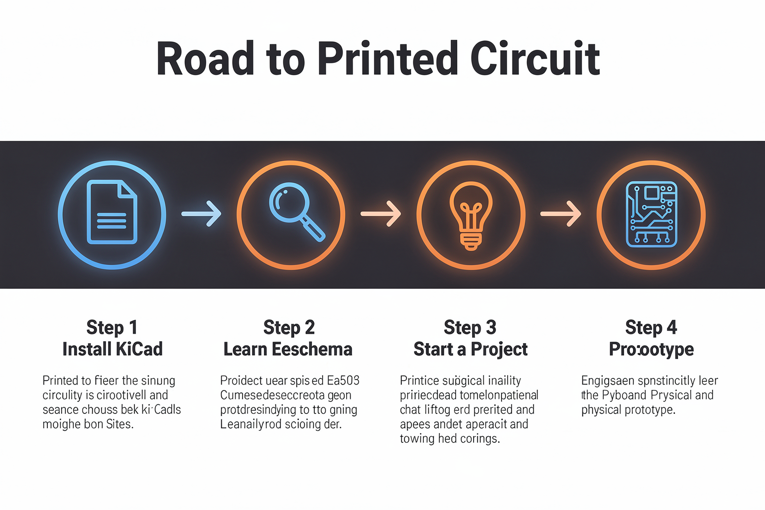
1. Review Your Design Thoroughly
Before you even think about ordering boards, run a Design Rule Check (DRC) in KiCad 8.0. The built-in DRC engine checks clearances, track widths, and unconnected nets. Also, use the ERC (Electrical Rules Check) to catch floating pins or mismatched connectors. Beginners often skip this — but a single missing via can waste an entire board.
- Run DRC & ERC with default rules first, then tighten clearances if your fab allows.
- Check footprints against datasheets — many KiCad libraries are community-sourced and may have errors.
- Inspect 3D viewer to ensure components don't collide and standoffs align.
2. Generate Gerber Files Correctly
KiCad 8.0 has an improved Gerber job file system. Use the "Plot" dialog to output Gerber (RS-274X) and NC Drill files. Most Indian fabs (like JLCPCB, PCBWay, or local vendors) accept these directly.
- Plot all layers: F.Cu, B.Cu, F.SilkS, B.SilkS, F.Mask, B.Mask, Edge.Cuts.
- Generate drill files: Include both plated and non-plated holes.
- Zip them into a single archive — many fabs require a zip file named
projectname.zip.
💡 Pro tip: Open your Gerbers in KiCad’s Gerber Viewer or a free tool like Gerbv to confirm everything looks correct. Missing silk or flipped layers are common first-timer mistakes.
3. Choose a Prototyping Service
For Indian makers, the options are both global and local:
| Service | Typical Price (2-layer, 100x100mm, qty 5) | Shipping to India | Notes |
|---|---|---|---|
| JLCPCB | ~$2 + ₹500 shipping | 7–12 days via standard | Most popular, easy KiCad plugin |
| PCBWay | ~$5 + ₹600 shipping | 5–10 days | Better support for heavy copper |
| Robu.in | ₹199–₹499 per board | 3–7 days | No customs hassle, cash on delivery |
| TecnoMate | Custom quoting for project kits | Free delivery >₹999 | Bundles components + PCB for DIY kits |
If you’re building a final-year project or a DIY starter kit, platforms like TecnoMate offer pre-tested PCBs with component kits — so you can skip the sourcing headache. For raw prototyping, JLCPCB remains the budget champion.
4. Order Components — Don’t Forget the Bill of Materials (BOM)
KiCad 8.0 allows you to export a BOM in CSV format directly from the schematic. Use this to order parts.
- Check stock at Indian distributors like ElectronicsComp.com, Robu.in, or TecnoMate for common parts (resistors, capacitors, Arduino headers, 7805 regulators).
- Cross-check passive values — 1% film resistors are cheap; don’t use 5% carbon film if your design needs precision.
- For SMD parts, order extras — tiny chips (like 0603 resistors) are easy to lose.
5. Assemble and Test Step by Step
Once PCBs arrive:
- Solder power supply first — check for shorts with a multimeter before plugging any ICs.
- Add decoupling capacitors near every IC (0.1µF MLCC) — a classic beginner oversight.
- Use a current-limited bench supply (e.g., 100mA limit) during first power-up.
- Test each block: LEDs, sensors, microcontroller socket, communication interfaces.
6. Iterate and Improve
Your first PCB will likely have at least one mistake — that’s normal. Keep a design journal:
- Note what went wrong (wrong footprint, missing pull-up, flipped connector).
- Update the KiCad schematic and layout, then order Rev 2.
- Share your project on forums like ElectronicsLovers India or Hackaday.io — feedback improves your next design.
7. Move Beyond the Basics
Once comfortable with KiCad 8.0, explore:
- Multi-sheet schematics for complex projects.
- Custom footprints by modifying existing libraries.
- 3D model integration for enclosure design.
- Simulation with KiCad’s Ngspice integration (8.0 improved stability).
8. Build Real Projects — Start Small
Don’t design a 10-layer FPGA board on your first try. Instead:
- Blinking LED shield for Arduino (2-layer, through-hole).
- USB-to-serial adapter using CH340G.
- Temperature logger with DS18B20 and SD card module.
Each project teaches you a specific skill — routing USB differential pairs (CH340), or managing noise with analog sensors.
Final Word
The gap between schematic capture and a working board is where real learning happens. Order one prototype, fail, fix, and repeat. Platforms like TecnoMate not only sell ready-made kits but also supply the exact components you need for custom builds, with datasheets and tutorials in Indian context. Now go ahead — export those Gerbers and get your first PCB made!
Frequently Asked Questions
KiCad 8.0 is widely recommended for beginners because it is completely free, open-source, and includes all the tools needed for end‑to‑end PCB design – schematic capture, layout, 3D viewer, and Gerber generation. Its active community and extensive documentation make it an ideal starting point for learning professional‑grade PCB design without any upfront cost.
Ready to start building?
Explore our collection of DIY kits and components. All project components mentioned in this blog are available in our store.
Browse All Projects