


Introduction
PCB design has become an essential skill for every electronics engineer and hobbyist in India. Whether you're creating a simple Arduino-compatible board for your college project or designing a complex IoT device for your startup, understanding PCB design is crucial. KiCad 8, the open-source EDA (Electronic Design Automation) software, has emerged as a powerful and free alternative to expensive commercial tools like Altium Designer or Eagle. This comprehensive guide will walk you through the complete PCB design workflow in KiCad 8, from schematic creation to generating manufacturable Gerber files, all while keeping in mind the Indian market context and budget constraints.
The beauty of KiCad lies in its accessibility - no licensing fees, powerful features, and an active community. For Indian engineering students and DIY enthusiasts watching every rupee, KiCad offers professional-grade capabilities without burning a hole in your pocket. In this guide, we'll explore each step of the PCB design process, share practical tips specific to Indian manufacturing capabilities, and help you transition from schematic to final Gerber files ready for fabrication.
Prerequisites: Setting Up Your Design Environment
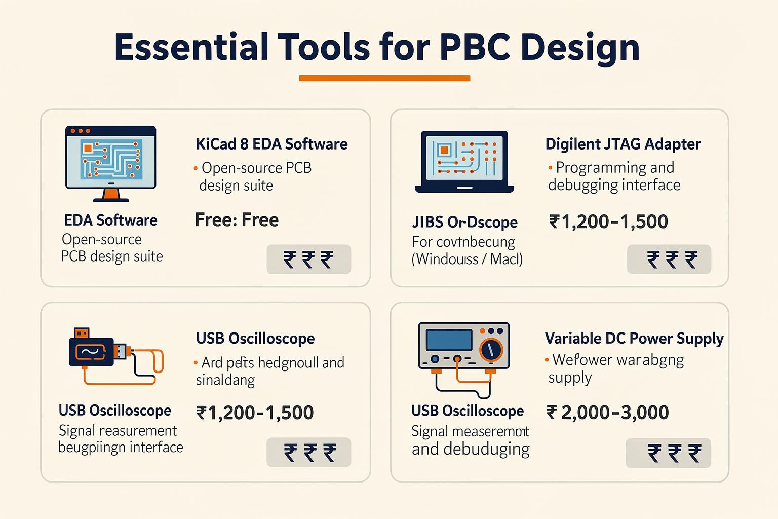
Before diving into PCB design, you need to ensure you have the right tools and components available. Based on Indian market availability and pricing, here's what you'll need:
| Component | Specification | Price (₹) |
|---|---|---|
| KiCad 8 Software | Open-source EDA suite | Free |
| Computer | Windows/Linux/Mac | As per your budget |
| Digilent JTAG Adapter | For programming microcontrollers | 1,200 - 1,500 |
| USB Oscilloscope | 100MHz+ basic model | 2,000 - 3,000 |
| Power Supply | Variable DC bench supply | 3,000 - 5,000 |
| Multimeter | Digital with continuity | 500 - 1,000 |
| Component Storage | Anti-static storage box | 200 - 400 |
| Breadboard | 400 tie-points | 150 - 250 |
Software Installation Guide
Setting up KiCad 8 is straightforward, but here are some specific tips for the Indian context:
-
Download from Official Source: Visit kicad.org and download the latest version. For better performance in India, consider using mirrors hosted in Asia if the main server is slow.
-
Install with Admin Rights: On Windows systems (common in Indian colleges), right-click the installer and select "Run as administrator" to avoid permission issues.
-
Library Installation: KiCad uses libraries for components. These are automatically downloaded when you first access the symbol or footprint editors.
-
Customizing PCB New Project Defaults:
CodeTecnoMatePreferences -> Configure Paths -> Set default footprint library path Preferences -> Configure Paths -> Set custom symbols library path
Hardware Setup for Testing
Having the right hardware for testing your designs is crucial, especially in the Indian context where local availability varies. Start with basic tools like a USB power supply (₹200-₹400), basic multimeter (₹500-₹1000), and a prototyping board (₹150-₹250). These tools will help you validate your designs before committing to PCB fabrication.
Getting Started: Creating Your First Schematic
A schematic is the blueprint of your electronic circuit. It shows the electrical connections between components but not their physical layout. Here's how to create your first schematic in KiCad 8:
Opening KiCad and Creating a New Project
- Launch KiCad 8
- Click "New Project" or go to
File -> New Project - Name your project (e.g., "Blinky_LED_Demo")
- Choose a location (save it to your Documents folder for easy access)
Setting Up the Schematic Sheet
- In the Schematic Editor window, click the "Add sheet" icon (looks like a page with a plus sign)
- Default sheet is named "sch1" - you can rename it to "Schematic"
- Set the grid size:
Preferences -> Grid Settings -> Set grid to 100 mil (2.54mm)
Adding Components to Your Schematic
- Open the component library selector (click the dropdown next to the search bar)
- Select "All footprints" to see all available components
- Search for components using:
- Resistors: Type "resistor" in the search box
- Capacitors: Type "capacitor"
- LEDs: Type "led"
- Microcontrollers: Type "atmega328" or "esp32"
Here's a practical example of adding a simple LED blinker circuit:
# Python script to generate component list for LED blinker
components = [
    {"value": "10k", "footprint": "Resistor_ThroughHole_Vertical", "ref": "R1", "pins": "2"},
    {"value": "220", "footprint": "Resistor_ThroughHole_Vertical", "ref": "R2", "pins": "2"},
    {"value": "LED", "footprint": "LED_ThroughHole_THT", "ref": "LED1", "pins": "2"},
    {"value": "16MHz", "footprint": "Crystal_HC49US", "ref": "XTAL1", "pins": "2"},
    {"value": "10uF", "footprint": "Capacitor_Electrolytic_Radial", "ref": "C1", "pins": "2"}
]
Wiring Your Circuit
- Select the "Place Wire" tool (shortcut: W)
- Click on component pins to route wires
- Avoid crossing wires when possible (KiCad will automatically add connection dots where wires cross)
- Add power and ground symbols for clarity
Annotating Your Schematic
Proper annotation is crucial for complex designs:
- Select
Tools -> Annotate Schematicor pressCtrl+Shift+A - KiCad assigns reference designators (R1, R2, C1, etc.)
- Check for duplicate designators
- Verify all components have unique references
Electrical Rules Check (ERC)
Before moving to the PCB layout, run ERC to catch potential errors:
- Select
Inspect -> Run Electrical Rules Check - Review the error report
- Fix issues like:
- Unconnected pins
- Pin conflicts
- Power pin issues
- Missing power connections
PCB Layout: From Schematic to Physical Design
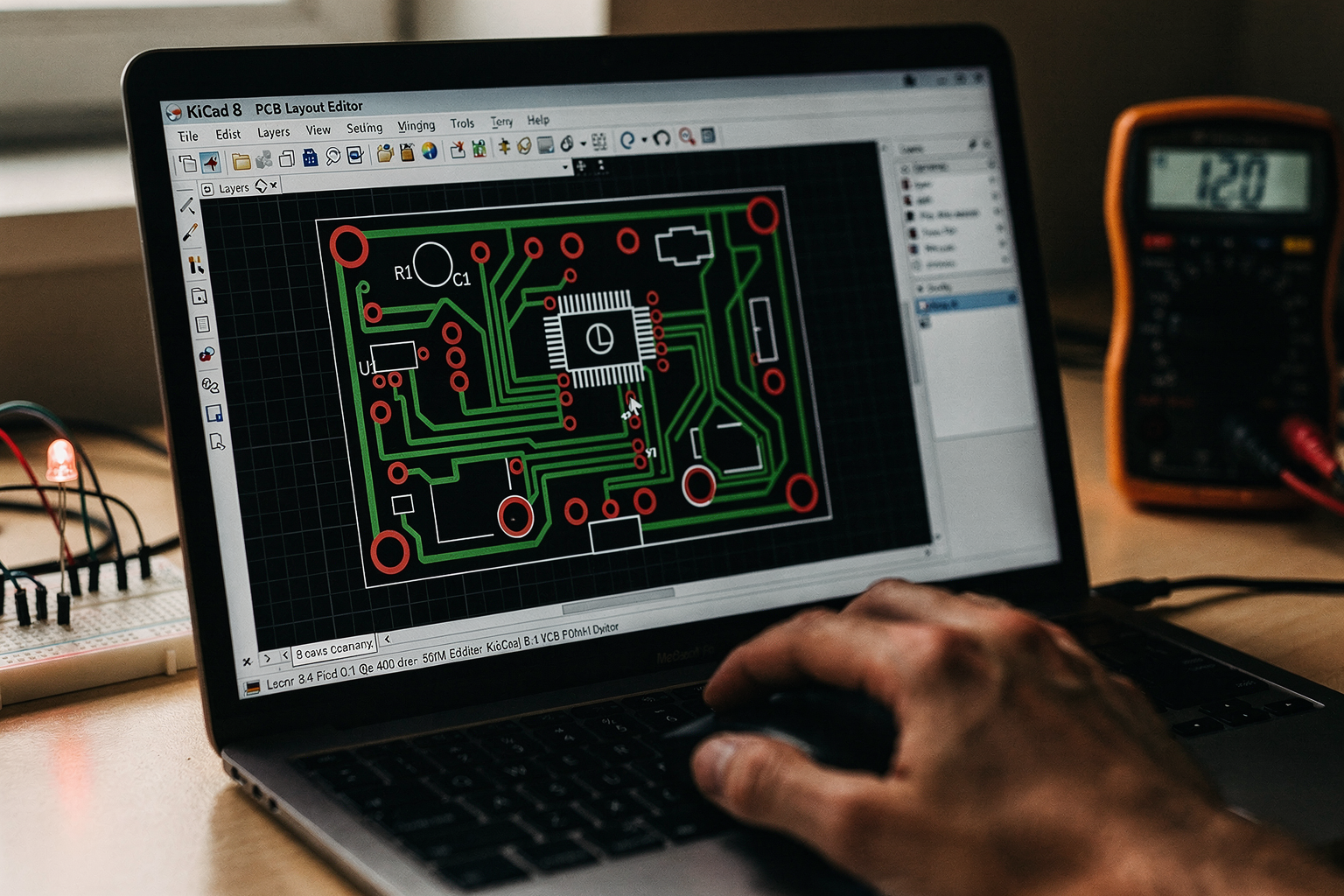
Now that your schematic is complete, it's time to create the physical PCB layout. This is where your circuit comes to life.
Setting Up the PCB Editor
- Double-click on the "sch1" sheet in the schematic editor
- The PCB editor will open with your footprint links
- Go to
File -> Load Footprint Linkif not loaded automatically
Board Properties and Setup
- Open board properties:
File -> Board Properties - Set your board outline:
- Width: 50mm
- Height: 70mm
- Configure design rules:
- Track width: 0.25mm (standard 1oz copper)
- Via size (drill): 0.8mm
- via size (pad): 1.0mm
Importing Schematic Data
- In the PCB editor, ensure your schematic is linked
- All components appear with their footprints
- Missing footprints appear as "?" - you'll need to assign them
Placing Components
Follow these placement principles for optimal PCB design:
- Group related components: Keep ICs near their peripheral components
- Consider component height: Place taller components away from connectors
- Thermal considerations: Leave adequate space for heat dissipation
- Manufacturability: Ensure sufficient clearance for soldering
Routing Your PCB
This is the most critical phase of PCB design. Here are some best practices:
Traces and Widths
# Standard trace widths for different applications
# (inmm)
ground_plane_width = 1.0  # Power and ground connections
signal_trace_width = 0.2  # General signal traces
power_trace_width = 0.5   # Power distribution

# DRC-friendly traces
high_current_trace = 1.0  # For motors, LEDs
Routing Techniques:
-
Ground Plane: Use
Shift+Gto toggle ground plane display- Fill large empty areas with copper (right-click -> Fill all zones)
- Connect to ground components via thermal reliefs
-
High-Speed Signals: Keep routing short and direct
- Avoid sharp 90-degree angles (use 45-degree angles)
- Maintain consistent trace spacing
-
Differential Pairs: Use
Alt+Dto highlight and route pairs together
Via Placement
- Use through-hole vias for power connections (more reliable)
- Place thermal vias under components with high power dissipation
- Connect ground planes with multiple vias for better grounding
Design Rule Check (DRC)
After routing, always run DRC to catch layout errors:
- Select
Inspect -> Design Rules Check - Review and fix these common issues:
- Clearance violations
- Track width violations
- Unconnected thermal pads
- Missing annular rings
3D Viewer
Use the 3D viewer to check for physical conflicts:
- Click the 3D viewer icon in the toolbar
- Rotate and zoom to check component clearance
- Verify height clearances for connectors and heat sinks
Generating Gerber Files: From Design to Manufacturing
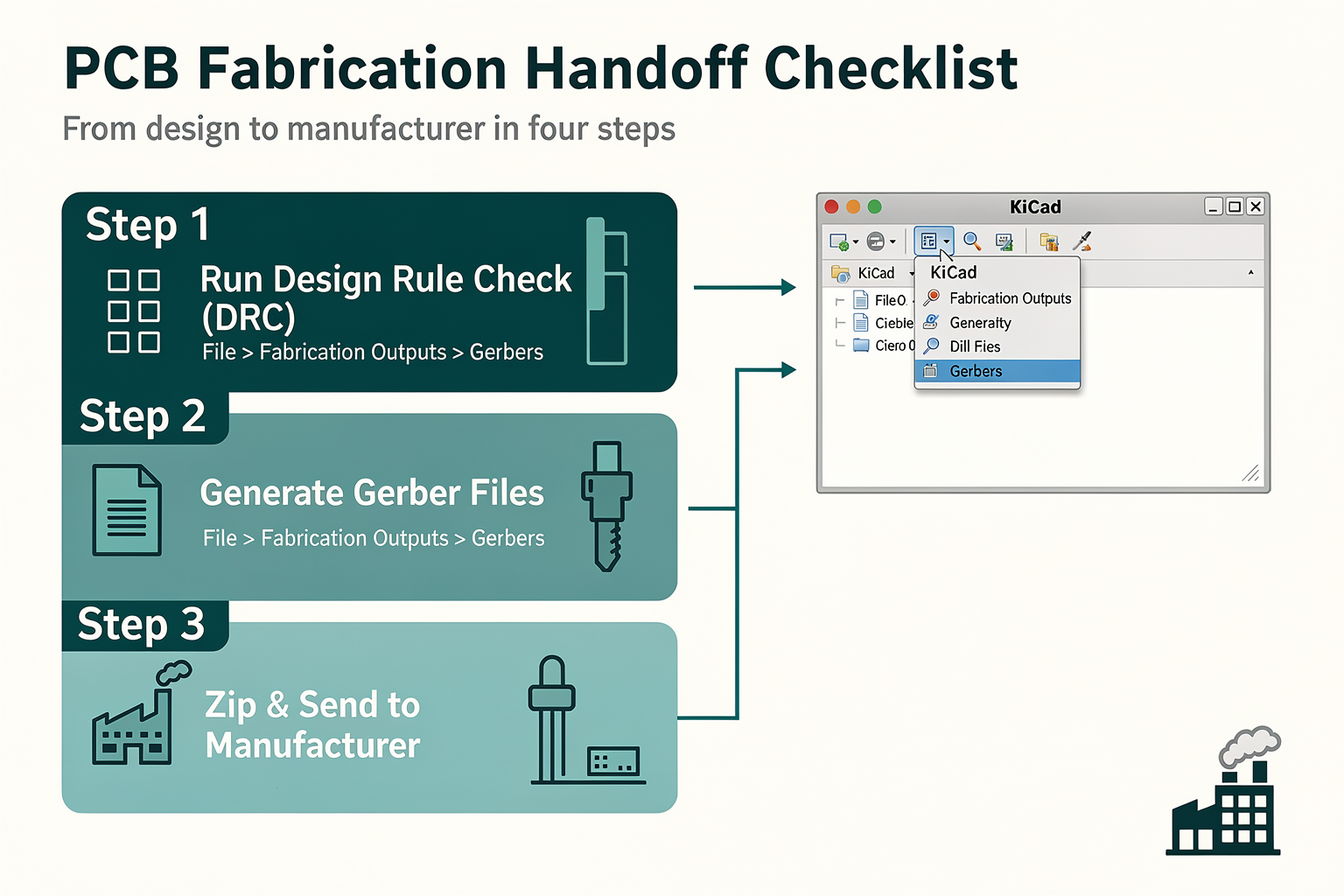
Gerber files are the industry standard format for PCB fabrication. Here's how to generate them in KiCad 8:
Output Job File Setup
- Select
File -> Plot - Click "Configure..." to open the Output Job File dialog
- Configure output options:
# Example Gerber generation settings for a 4-layer board
# Layers:
# 1 - Top Copper
# 2 - Inner Ground
# 3 - Inner Power
# 4 - Bottom Copper

Gerber files to generate:
- Copper layers: F.Cu, In1.Cu, In2.Cu, B.Cu
- Solder mask: F.Mask, B.Mask
- Silkscreen: F.SilkS, B.SilkS
- Solder paste: F.Paste
- Drill files: Excellon drills
- Fabrication drawing: Dwg
Configuring Plot Settings
For each layer, configure:
-
Copper Layers:
- Mode: Copper
- Scale: 1.0 (or 2.0 for mirrored layers)
- Origin: Bottom Left
-
Solder Mask:
- Mode: Solder Mask
- Use drill file: Yes
- Minimum clearance: 0.05mm
-
Silkscreen:
- Mode: Silkscreen
- Color: White
- Minimum width: 0.1mm
Generating Drill Files
- Select
File -> Plot/Gerber Files...-> Configure - Enable "Generate drill files"
- Set format to "Excellon drill files"
- Choose "Generated drill file format"
Generating Fabrication Drawing
- In the Output Job File dialog, enable "Plot fabrication drawing"
- Configure:
- Plot outline: Checked
- Plot dimensions: Checked
- Plot reference designators: Checked
- Plot sheet: Checked
Final Output Organization
Create a professional output structure:
project_name/
├── gerber/
│   ├── copper/
│   │   ├── F.Cu.gbr
│   │   ├── In1.Cu.gbr
│   │   ├── In2.Cu.gbr
│   │   └── B.Cu.gbr
│   ├── solder_mask/
│   │   ├── F.Mask.gbr
│   │   └── B.Mask.gbr
│   ├── silkscreen/
│   │   ├── F.SilkS.gbr
│   │   └── B.SilkS.gbr
│   ├── drill/
│   │   └── drill_report.csv
│   └── fabrication.drl
└── fabrication_drawing.pdf
Troubleshooting Common PCB Design Issues
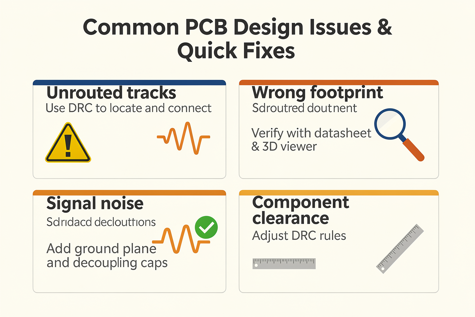
Even experienced designers encounter problems. Here's a troubleshooting guide specific to common issues in KiCad:
| Issue | Symptoms | Solution |
|---|---|---|
| Missing footprints | Footprints show as "?" | Use Footprint Selector to assign correct footprint from library |
| ERC errors | Unconnected pins, power issues | Run ERC, fix each warning, re-run until clean |
| DRC violations | Track clearance errors | Adjust routing, increase clearance, check rules settings |
| Silkscreen overlap | Text overlapping copper | Move silkscreen using Ctrl+M to move, or adjust grid |
| 3D viewer errors | Component collision warnings | Redesign component placement, check height values |
| Gerber file issues | Missing layers or corrupted files | Verify all layers are plotted in Output Job File |
Common Pitfalls and How to Avoid Them
-
Power Issues:
- Always use proper power symbols (VCC, GND)
- Check power rails in the schematic
- Verify power connections in the layout
-
Signal Integrity:
- Keep high-speed signals short and direct
- Avoid routing under ICs
- Use proper ground planes
-
Manufacturing Considerations:
- Minimum trace width: 0.1mm for 1oz copper
- Minimum clearance: 0.1mm between copper features
- Avoid 4-layer boards if not required (cost increases significantly)
Indian Manufacturing Specific Tips
-
Panelization: Most Indian manufacturers prefer panelized boards for cost efficiency
-
Material: Standard FR4 with 1.6mm thickness is most common and cost-effective
-
Copper Weight: 1oz (35μm) copper is standard; 2oz for high-current applications
-
Surface Finish: HASL (Lead-Free) is standard and cost-effective in India
Advanced Tips for Professional PCB Design
Creating Custom Libraries
For components not in standard KiCad libraries:
# Python script to create custom component library
import kicad

def create_custom_resistor(value, footprint, reference):
    component = kicad.Symbol(reference)
    component.add_property("Reference", reference)
    component.add_property("Value", value)
    component.set_footprint(footprint)
    return component

# Usage
custom_res = create_custom_resistor("100k", "Resistor_SMD_0603", "R1")
Batch Processing with Python Scripts
Automate repetitive tasks using Python scripting:
# Example script to batch update component values
import kicad

def update_all_resistors(new_value):
    for symbol in project.get_symbols():
        if symbol.get_property("Device") == "Resistor":
            symbol.set_property("Value", new_value)

# Update all resistors to 10k
update_all_resistors("10k")
Using Templates for Consistency
Create project templates for common designs:
- Save frequently used component configurations
- Create standard board outlines for common applications
- Develop custom schematic symbols for frequently used components
Design for Assembly (DFA) Tips
- Component Orientation: Align similar components in the same direction
- Test Points: Add test points for critical signals (VCC, GND, clock)
- LED Placement: Position LEDs for easy visibility
- Connector Accessibility: Ensure connectors are accessible for programming and testing
Frequently Asked Questions
Most Indian PCB manufacturers like PCB Power, Circuits Corporation, and others can fabricate boards as small as 50x50mm. For single-sided boards with 4 layers, typical costs range from ₹300-₹800 depending on complexity and quantity. Prototype quantities (1-5 boards) usually cost 2-3x more than bulk orders.
Ready to start building?
Explore our collection of DIY kits and components. All project components mentioned in this blog are available in our store.
Browse All Projects